Observation of a Kekulé vortex in graphene
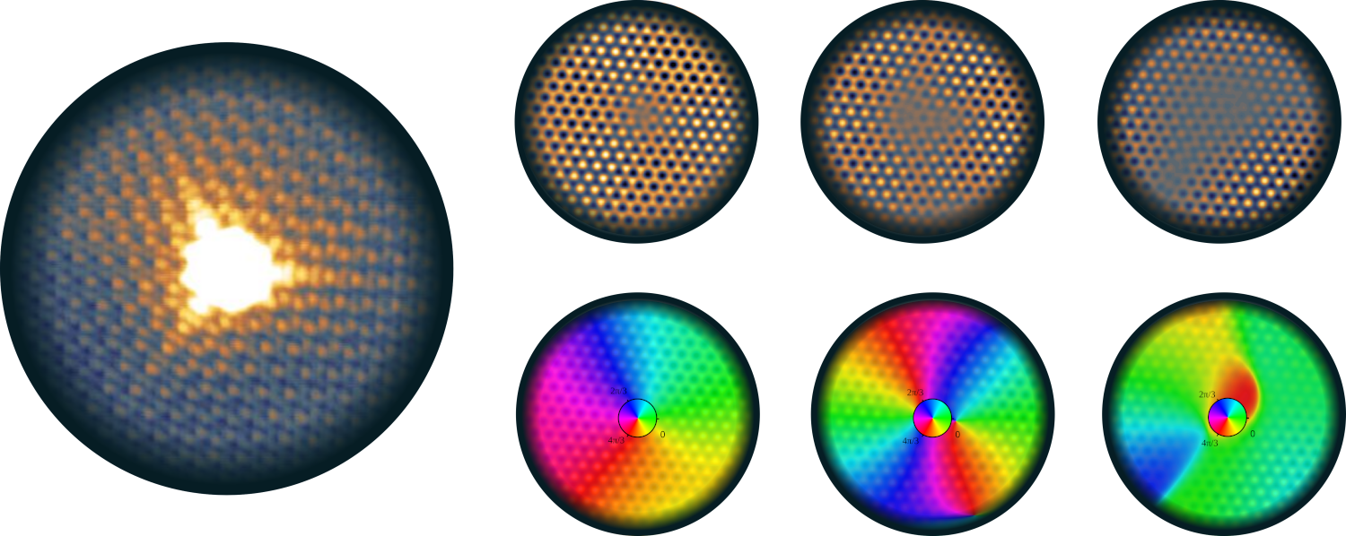
Fractional charges are one of the wonders of the fractional quantum Hall effect. Such objects are also anticipated in two-dimensional hexagonal lattices under time reversal symmetry—emerging as bound states of a rotating bond texture called a Kekulé vortex. However, the physical mechanisms inducing such topological defects remain elusive, preventing experimental realization. Here, we report the observation of Kekulé vortices in the local density of states of graphene under time reversal symmetry. The vortices result from intervalley scattering on chemisorbed hydrogen adatoms. We uncover that their 2π winding is reminiscent of the Berry phase π of the massless Dirac electrons. We can also induce a Kekulé pattern without vortices by creating point scatterers such as divacancies, which break different point symmetries. Our local-probe study thus confirms point defects as versatile building blocks for Kekulé engineering of graphene’s electronic structure..
Référence : Y. Guan in Nature Commun. 15, 2927Here (2024).Giant Atomic Swirl in Graphene Bilayers with Biaxial Heterostrain.
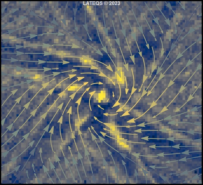
We report a new type of moiré superlattice in bilayer graphene. The superlattice does not originate from twist between the layers but from biaxial heterostrain. Here one layer is strained with respect to the other. In our experimental implementation biaxial heterostrain is small (~0.1%) and the superlattice is huge ~250 nm in period so that the system relaxes to a more favourable configuration where strain is confined in narrow spiraling 1D regions hosting topological electronic states. Graphene bilayers with biaxial heterostrain therefore offers a new playground for moiré physics in graphene.
Référence : Advanced Materials Here (2023).Heterostrain rules the flatbands in twisted graphene layers.
The strongly correlated electron physics recently observed in twisted graphene layers develops in flatbands which are very sensitive to the relative arrangement between the layers. For instance, the
superconducting phase has been reported to occur in a very narrow range of rotation angle between the layers around the magic angle. ...
As another illustration, hydrostatic pressure changes the interlayer distance which
also strongly influences superconductivity. Heterostrain, the in-plane deformation of one layer with respect to the other is an ubiquitous source of modification of the relative arrangement between the layers. Experiments and theory have shown that heterostrain affects the flat bands which could have an
impact on the strongly correlated electron physics. Bi, Yuan and Fu have even predicted that near the magic angle, the bandwith becomes insensitive to the twist angle and that the effect of heterostrain is dominant, calling
for systematic experimental study of its effect. Such program is however difficult to implement owing to the lack of controllability of heterostrain, and its inhomogeneity sometimes referred to as ”twist angle disorder” and which
was also found to impact strongly correlated states at the macroscopic scale. In order to overcome these issues, we survey already published experimental STM data in view of quantifying the effect of homogeneous heterostrain on the physics of magic-angle twisted
graphene layers. We show that heterostrain is indeed the main structural parameter determining the flatbands in magic angle twisted graphene layers.
More info in F. Mesple et al. in Phys. Rev. Lett. 127, 126405 (2021).
Measuring the Berry phase of graphene at B=0T.
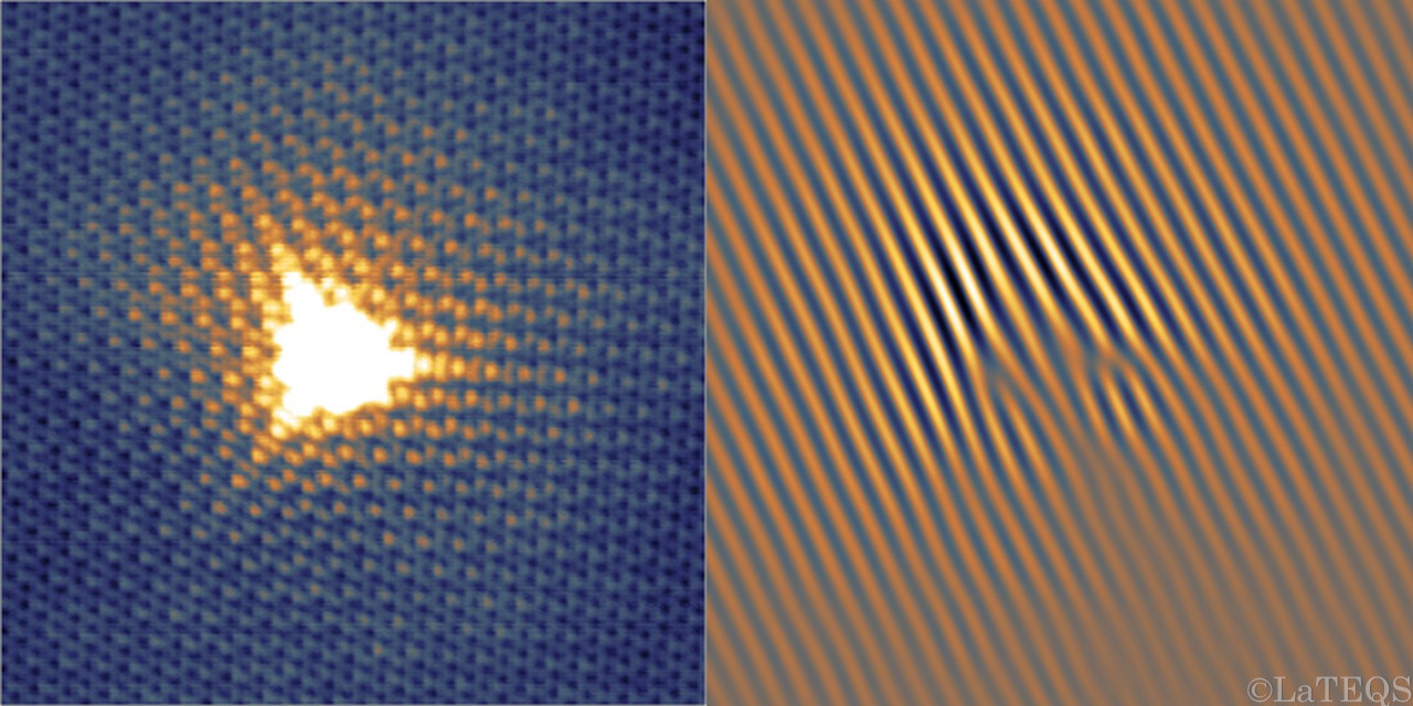
The ultra-relativistic nature of electrons in graphene relates to a topological property of their wave-functions. We have proposed a new scanning tunneling microscope approach to measure this topological property
in the electronic density near an hydrogen atom grafted on the surface. ...
Time zone is a useful way to represent time at the surface of the globe. However, it rises the following question : what time is it at the North pole where all the time zones meet? Within this representation,
the North pole is a singular point where time is not well defined. A way to reveal this singularity is to send a traveler circumnavigating the globe to the East like Jules Vernes’ Phileas Fogg in his book ‘Around the World in Eighty Days’.
The traveler crosses the 24 time zones during his journey. Switching his watch one hour forward each time he crosses a time zone, he will observe a time shift of exactly one day as his returns to the starting point compared to
an observer who remained there. This difference which is the key to the final twist in Vernes’ book is remarkable in that it does not depend on the details of the travel such as the latitude.
It depends only on the number of turns around the north pole. Such a property is said to be topological.
In quantum physics, topological properties characterize new electronic states. For instance, low energy electrons in graphene behave as particle moving close to the speed of light.
This ultra-relativistic behaviour is characterized by a topological singularity, some sort of North pole in an abstract space. Since electrons also have clocks (the phase of their wavefunction),
the topological singularity has been revealed by forcing the electrons to loop around it with magnetic fields and by comparing their clocks. Under these conditions, the phase difference acquired
after the navigation led to the observation of the anomalous Quantum Hall Effect, which confirmed the existence of ultra-relativistic particles in graphene.
We have presented a new approach to access the same topological property. The method is a conceptual leap as it does not require to force electrons around their north pole. Instead, the researchers have shown
that it is possible to materialize the abstract singularity at the surface of graphene by grafting an hydrogen atom on it. This is unveiled by wavefront dislocations in the local density of electrons near the
hydrogen atom observed in Scanning Tunneling Microscope images (figure above). They showed that the number of additional wavefronts is a measure of graphene’s singularity. This discovery opens a new route to understand
the topological state of matter, which determine the optical and electronic properties of materials.
More info in C. Dutreix et al in Nature 574 2019 (2019).
Heterostrain in twisted graphene layers
A variety of new electronic, optoelectronic and photovoltaic devices are produced by stacking different two-dimensional materials into van der Waals heterostructures.
Radical effects on the electronic properties ... can also be achieved by stacking identical materials into van der Waals homostructures. The properties of van der Waals structures and device not only depend on
the choice of materials but also on the details of the stacking which offers additional degrees of freedom. The rotation angle between the layers has been the first to be exploited exploited leading to the
discovery of a loarge amount of new physics :van Hove singularities in twisted graphene layers (TGLs) the Hofstadter butterfly in graphene on h-BN and very rencently to uncover correlated insulating and superconducting
states in magic angle twisted graphene layers. Strain, originating from external stress or from interlayer interactions, is another degree of freedom.
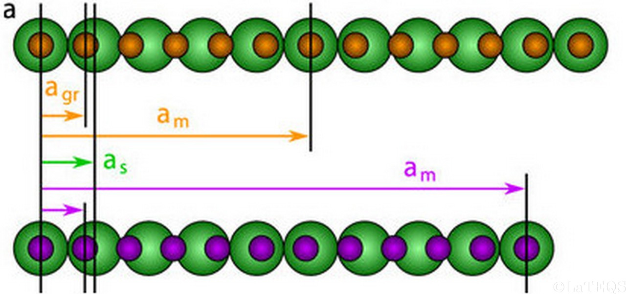
In the present work we have studied the effect of homogeneous heterostrain on electronic properties of TGLs.
Here, the layers experience different and independent homogeneous in-plane strain, a situation which has no equivalent in bulk materials where covalent bonds link atoms on both sides of the junction.
Heterostrain is possible in 2D stacks because independent deformations on each side of the interface are allowed by the weak interlayer van der Waals bonding. The top figure illustrates how heterostrain influences the
moiré between two rotated graphene layers.
Using our formalism to determine quantitatively heterostrain, we have shown that a tiny amount of heterostrain has strong implications for the electronic properties of twisted graphene layers.
In our case it lead to the formation of flat bands in which the strongly correlated electron physics could also develop.
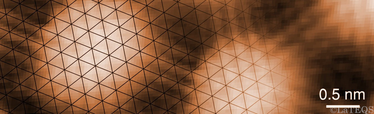
The following figure shows the STM image of the twisted graphene layers that we have studied and its density of states measured in spectroscopy mode. More info in L. Huder et al in Phys. Rev. Lett. 120 156405 (2018).
Epitaxial electrical contact to graphene
Surface electrical contacts to two-dimensional materials suffer from the poor coupling between the 2D surface and the 3D metal. The situation is further degraded by ...
contamination in the lithographic processing and/or layer transfer. The best innovation is the recent realization of one-dimensional edge-contacts to graphene possibly
combined with large doping. However, the improvement of contact resistance is made at the expense of technological simplicity since the contact fabrication necessitates
several steps.
 Edge bonding and large electron transfer are known to occur during the growth of graphene on SiC and could be exploited for electrical contacts if SiC was
replaced by a similar yet conducting material. Conducting carbides appear as good candidates since they have similar chemical properties and since they could allow new
functionalities owing to additional material properties such as magnetism or superconductivity.
Edge bonding and large electron transfer are known to occur during the growth of graphene on SiC and could be exploited for electrical contacts if SiC was
replaced by a similar yet conducting material. Conducting carbides appear as good candidates since they have similar chemical properties and since they could allow new
functionalities owing to additional material properties such as magnetism or superconductivity.
The growth of graphene on carbides other than SiC was first demonstrated by Foster, Long and Strumpf. In 1958, they showed that “aluminum carbide dissociates in the vicinity of 2200-2500 ◦ C, at atmospheric pressures, to aluminum vapor
and pure single crystals of graphite” establishing that other carbides could potentially be used for graphene technology. Nevertheless, this subject has remained unexplored
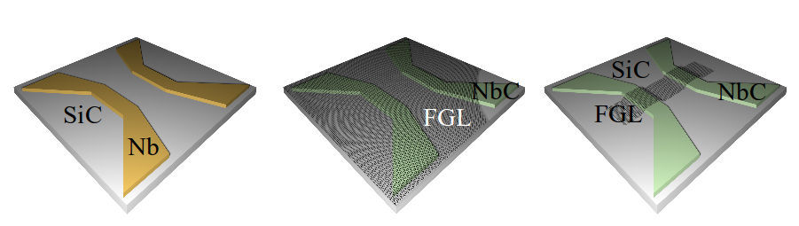
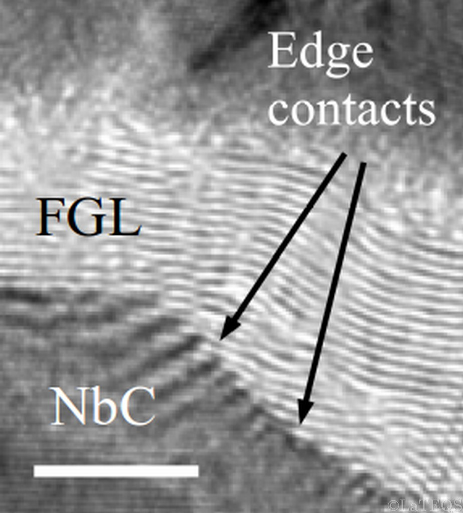
owing to the lack of commercial substrates. In this work, we have demonstrated that few graphene layer can be grown on a metallic carbide by thermal annealing of a carbide forming
metal film (niobium or tantalum) on SiC in high vacuum circumventing the problem of metallic carbide substrate availability. Based on this discovery we have described a resist-free
and scalable method to fabricate few graphene layers (FGL) with electrical contacts in a single growth step. The combined effect of edge-contact and partially-covalent surface
epitaxy between graphene and the metallic carbide allowed us to fabricate devices in which low contact-resistance and Josephson effect were observed.
More info in T. Le Quang et al in Carbon 121 48 (2017).
Classification of Moiré superlattices
A collaboration with Institut Néel (Grenoble)
The exotic electronic properties of pristine graphene are often altered when graphene is supported by a substrate. Indeed, due
to the structural mismatch between graphene and its support, graphene has ... periodically varying stacking configurations with its substrate. This effect
modulates the graphene-substrate interaction and distance, over a so-called moiré periodicity, which can range from ~1 to ~15 nm.
 The usual structural model used to describe moirés assumes
(Figure on the right top) that a single moiré beating occurs within a moiré period and that the graphene
and moiré lattices are commensurate (integer multiples of their lattice parameters can be found which are equal). Unfortunately, this simple model fails to explain
some experimental observation and more elaborate models have been developed. Some simply assume that the graphene and moiré lattices are incommensurate. Others assume commensurability,
yet without the constraint of a single moiré beating within the moiré unit cell (right figure bottom).
The usual structural model used to describe moirés assumes
(Figure on the right top) that a single moiré beating occurs within a moiré period and that the graphene
and moiré lattices are commensurate (integer multiples of their lattice parameters can be found which are equal). Unfortunately, this simple model fails to explain
some experimental observation and more elaborate models have been developed. Some simply assume that the graphene and moiré lattices are incommensurate. Others assume commensurability,
yet without the constraint of a single moiré beating within the moiré unit cell (right figure bottom).
There are many ways the above assumption for commensurability can be fulfilled, as can be shown by considering strains and rotation of the graphene with respect to its
substrate. Despite previous efforts, a comprehensive description of those effects was lacking. We have provided a fully-consistent description of the full complexity of commensurate
moiré superlattices, relating the graphene, substrate, and moiré, for the general case of an arbitrary strain (including shear, uniaxial, biaxial) and of superlattices having any
number of beatings. We have used this new description to to revisit previously published analysis of experimental observations. We have shown that supported graphene is subjected to strain
levels far below what is usually assumed.
More info in A. Artaud et al Sci. Rep 6 25670 (2016).
Superconducting Graphene
A collaboration with Institut Néel (Grenoble) and SIMaP (Grenoble)
The manifestation of superconductivity in graphene has been the topic of numerous recent theoretical works, which predicted new behaviors
in this 2D ballistic system ... where electrons are described by a relativistic equation. The integration of graphene into Josephson junctions has already
shown that a superconducting current could be measured across the carbon layer, but the good quality of the interface between graphene and a superconductor
remains very challenging and yet a key factor to study the superconducting proximity effect.
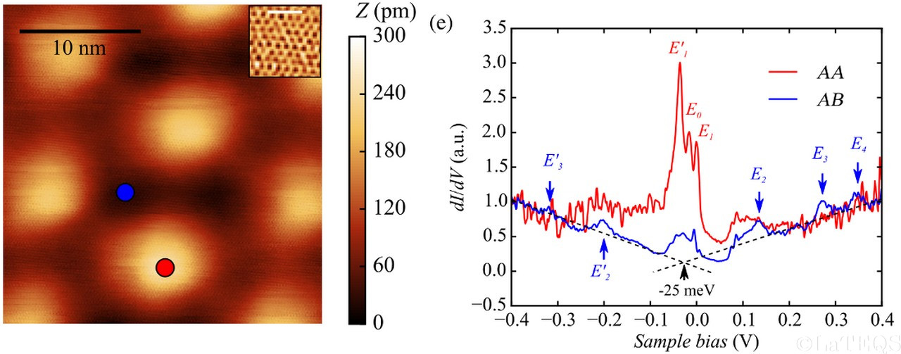
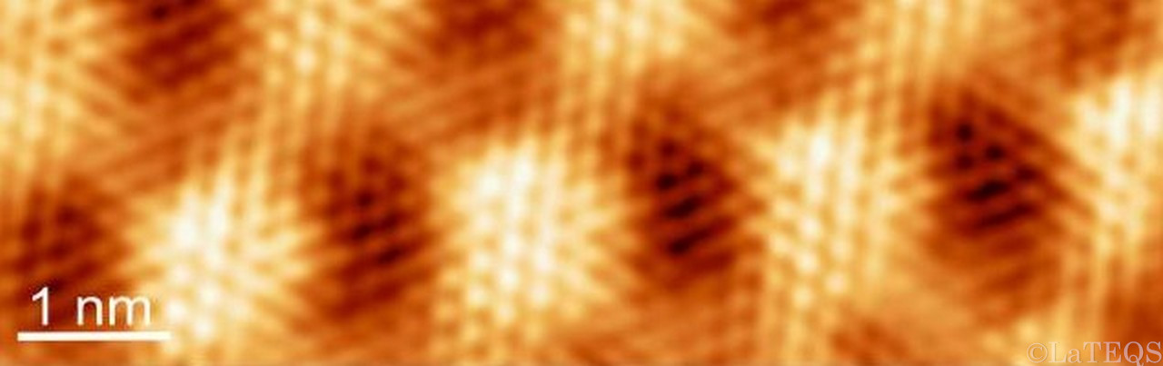
We developed a new very efficient way to strongly couple graphene to a superconductor, by growing it directly on top of rhenium, which shows superconductivity below 2K.
The graphene monolayer has been grown by a chemical vapor deposition process in a UHV chamber on epitaxial rhenium thin films of 30 nm thickness. The lattice parameters
mismatch between graphene and Rhenium gives rise to a so-called moiré pattern that we characterized by scanning tunneling microscopy (STM, cf figure below) and simulated
with ab initio calculations.
 The moiré supercell has a periodicity of 1.9nm +/- 0.1nm, which corresponds to eight carbon rings matching seven rhenium atoms. Our simulations
show the valleys correspond to regions where the graphene interacts strongly with the underlying substrate while the hills correspond to weaker interacting regions.
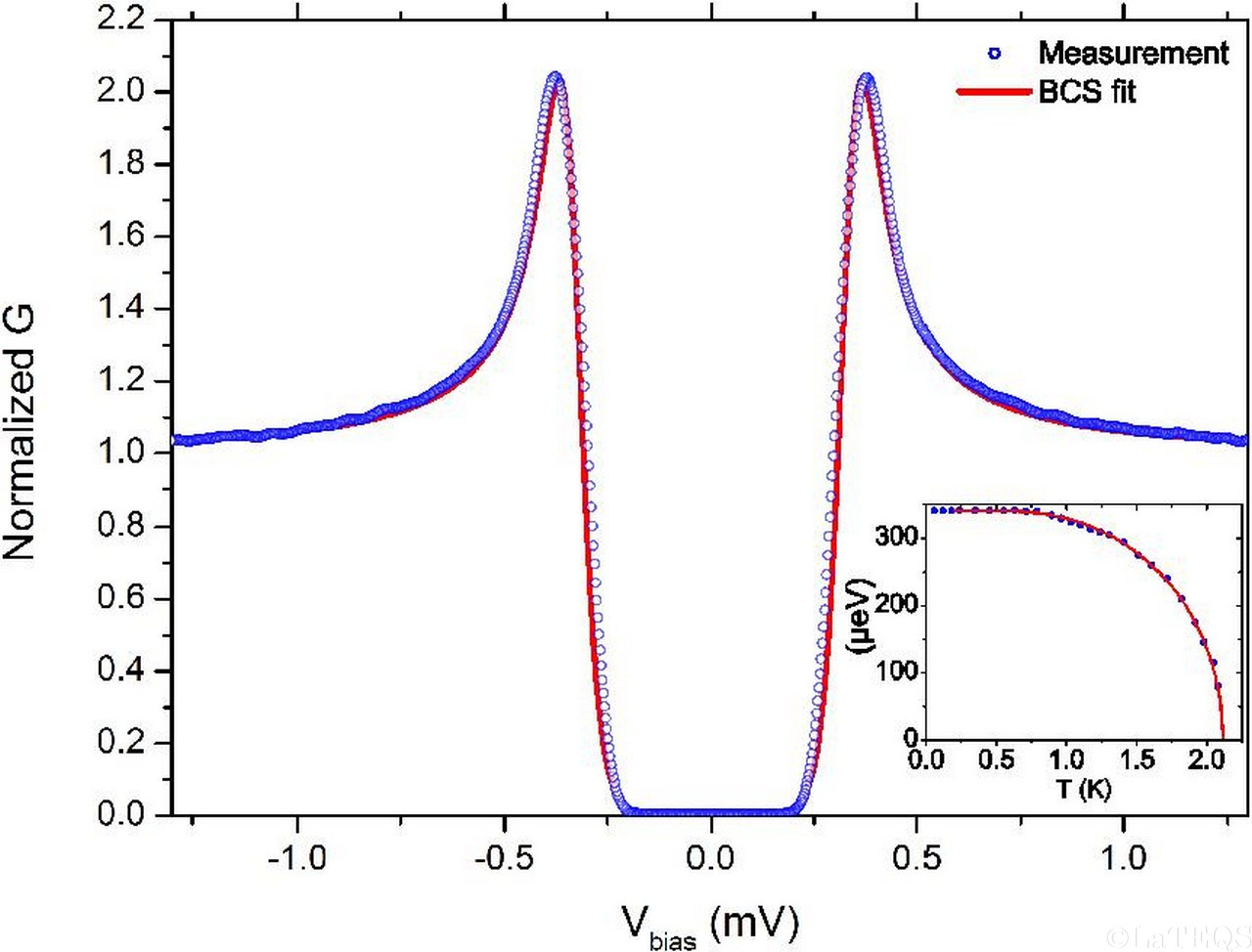
Spectroscopic measurements performed at 50mK revealed that the density of states around the Fermi energy is position dependent on the moiré and highlighted a
homogeneous superconducting state of the graphene layer, well fitted by the standard Bardeen-Cooper-Schrieffer (cf figure below). All our results demonstrate a
very good interface between graphene and the superconducting rhenium substrate, turning our system into a building block to design hybrid superconducting nanostructures,
where the good transparency of the superconductor-normal metal interface is of primary importance.
The moiré supercell has a periodicity of 1.9nm +/- 0.1nm, which corresponds to eight carbon rings matching seven rhenium atoms. Our simulations
show the valleys correspond to regions where the graphene interacts strongly with the underlying substrate while the hills correspond to weaker interacting regions.
Spectroscopic measurements performed at 50mK revealed that the density of states around the Fermi energy is position dependent on the moiré and highlighted a
homogeneous superconducting state of the graphene layer, well fitted by the standard Bardeen-Cooper-Schrieffer (cf figure below). All our results demonstrate a
very good interface between graphene and the superconducting rhenium substrate, turning our system into a building block to design hybrid superconducting nanostructures,
where the good transparency of the superconductor-normal metal interface is of primary importance.
Read more in C. Tonnoir et al. Phys. Rev. lett. 111, 246805 (2013)
Electric field-controlled rippling of graphene
A collaboration with Institut Néel (Grenoble)In the development of graphene based electronic devices a lot of care is usually taken in order to preserve its outstanding
electronic properties. The quality of the graphene itself and the absence of defects or contamination are at the heart of most
of the researches. A lot of efforts are also focused on ... the choice of the substrate which is known to play an important role. However,
these devices require the presence of metallic electrodes to connect it to the outside world. Very little is known about the impact of
these metallic contacts on the properties of graphene. In particular, the mechanical stress that is induced in graphene during the
metal thin film deposition can greatly influence the graphene properties near the contact and further limit the electronic mobility
of the global device.
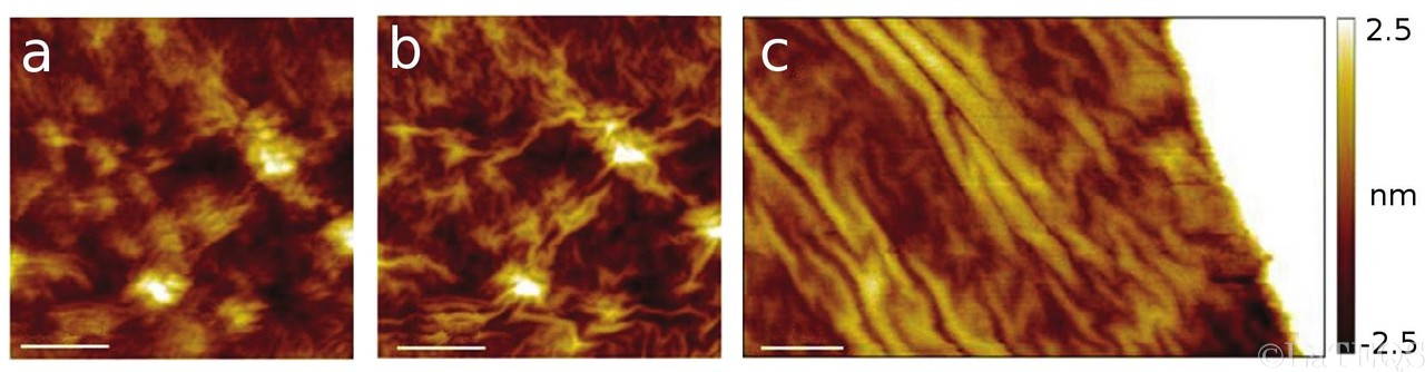
Ripples observed at different bias bias voltages Vb, 0.1 V and 0.5 V respectively, 250 nm away from the graphene-metal interface (a and b).
Closer to the metal layer (c), a strong buckling of graphene can also be observed which leads to wrinkles parallel to the graphene-metal interface.
This strained graphene display a gap of a few hundred of millivolts in the local electronic density of states
STM imaging and tunneling spectroscopy of graphene performed in the vicinity of a metallic film deposited on top of it, reveal intense
shear stress. They lead to a series of mechanical instabilities which take different morphologies as one comes closer to the metal
contact edges. In particular, for positions less than a micron away from the contact, we show a bias dependent rippling of graphene which
is enhanced by increasing the transverse electric field induced under the tip of the STM. (Fig. 1A & 1B) These ripples are suspended areas of
graphene which can be easily pulled by the STM electric field and therefore manipulated at will. In extreme situations, we observed a strong
buckling of graphene nearby the metallic electrode. (Fig. 1C)
br>
In this case tunneling spectroscopy reveals a gap of a few hundred millivolts in the local electronic density of states in
graphene. This gap can be explained by the interplay of quantum confinement and Coulomb blockade.
More info in Nanoscale DOI: 10.1039/C3NR02934D (2013).
